- Electrification
- Global
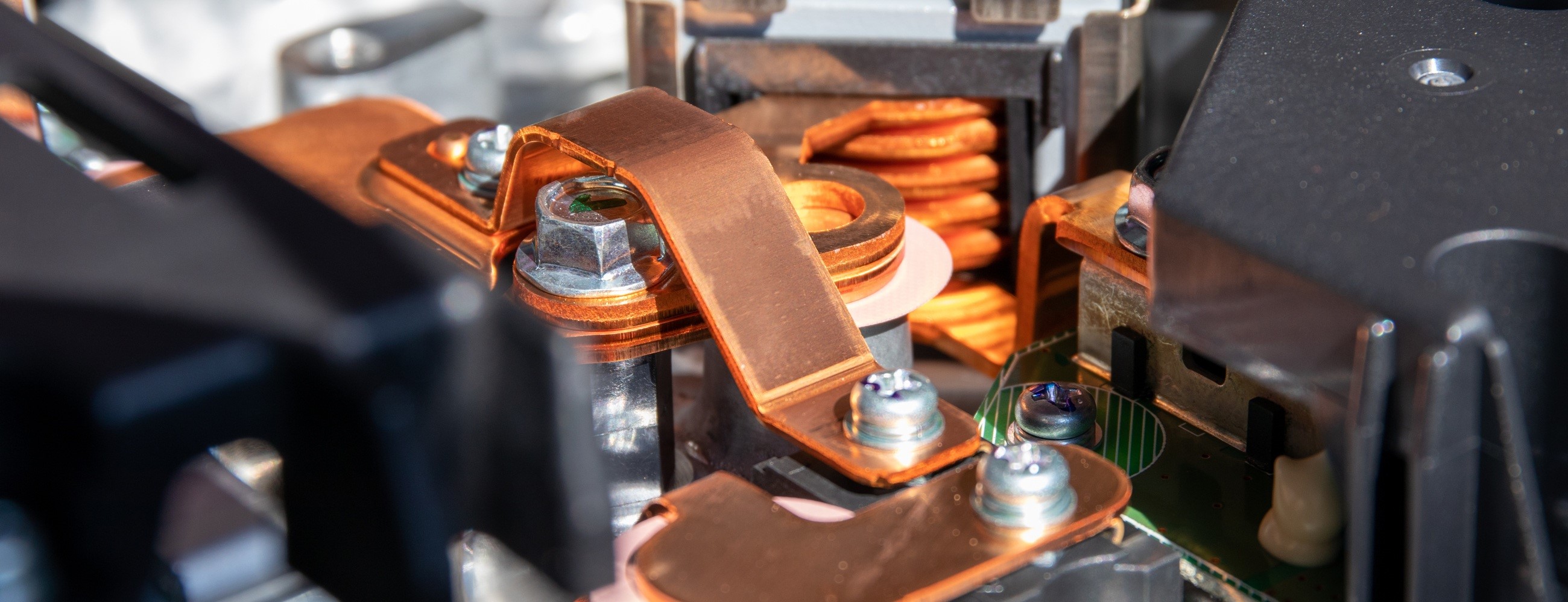
Insert Molding Technology for Low-Inductance Laminated Busbars
As power supplies and inverters continue to push toward higher efficiency and faster switching speeds—driven by the adoption of wide-bandgap semiconductors such as SiC and GaN— the parasitic inductance of wiring has become a critical design challenge. This article explains the fundamentals and applications of laminated busbars, the principles behind low-inductance design, and NAGASE Mobility’s insert molding technology used to achieve low-inductance busbar structures.
What Is a Laminated Busbar?
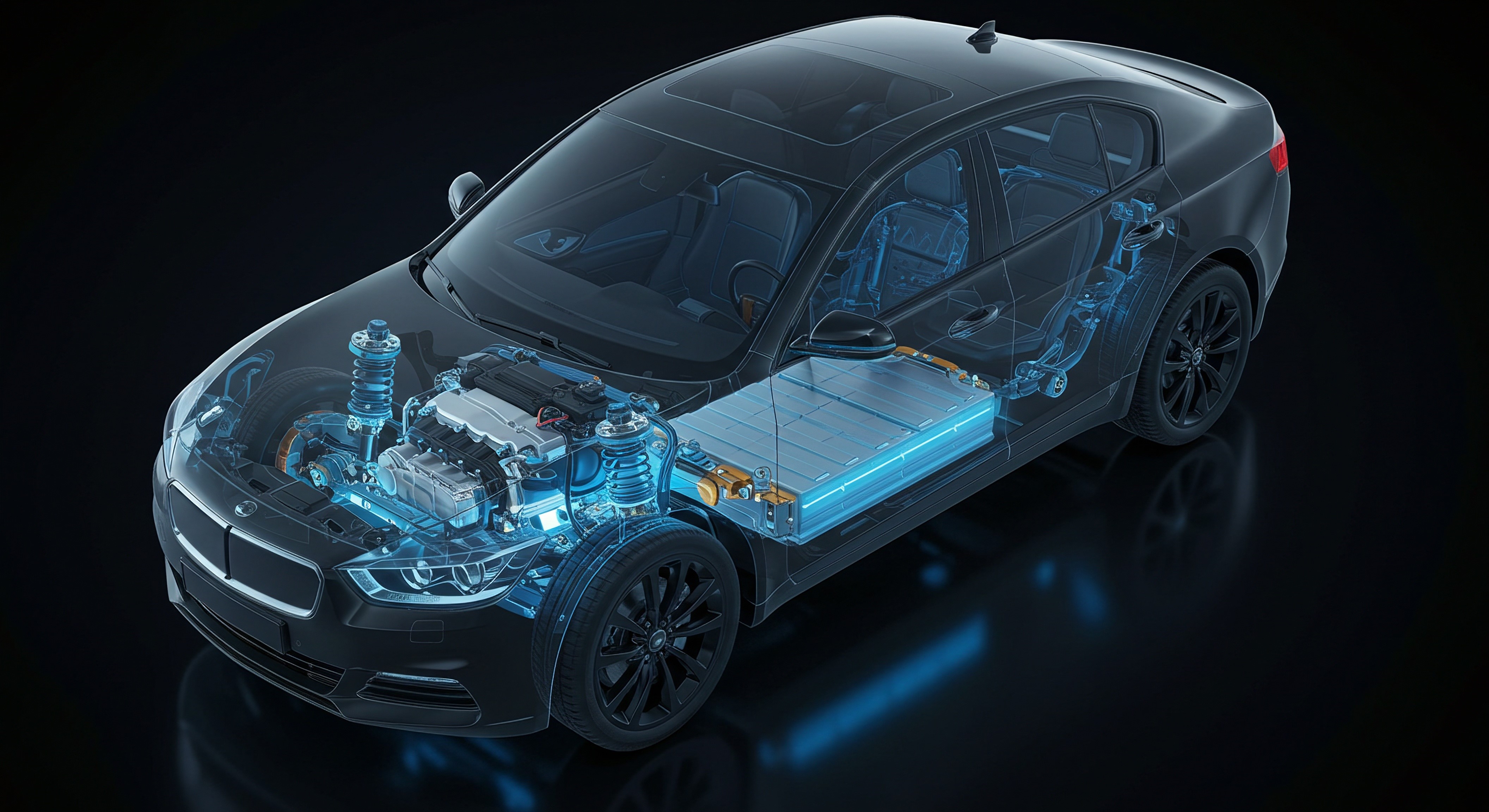
A laminated busbar distributes power by stacking multiple conductive plates—typically copper—separated by insulating materials. Laminated busbars are widely used in high-current and high-voltage power circuits, including inverters, DC-DC converters, and other power electronics systems.
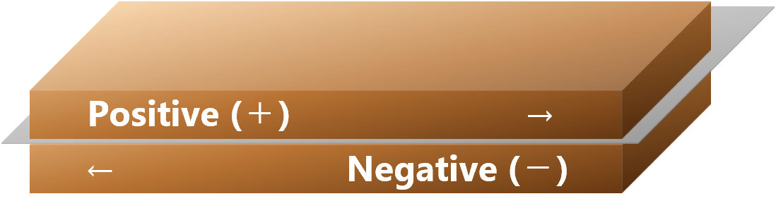
A key feature of laminated busbars is that the forward and return current paths can be placed close to each other. This structure reduces the current loop area and helps minimize parasitic inductance.
Difference from Single Busbars
Single busbars have a simpler structure than laminated busbars and are often chosen when minimizing manufacturing complexity is a priority. However, because the forward and return current paths are typically routed separately, the current loop area is larger.
As a result, parasitic inductance increases, potentially causing overvoltage during high-speed switching.
Difference from Cables
Cables are sometimes used for power distribution. However, busbars are generally preferred for power interconnections around power modules because they offer lower inductance and higher current-carrying capacity.
Cable wiring is flexible and easy to route, but the forward and return current paths tend to separate, which enlarges the current loop area. As a result, parasitic inductance rises, making overvoltage spikes and electromagnetic noise more likely during high-speed switching.
In contrast, laminated busbars stack conductive plates so that the forward and return current paths sit close together. This arrangement reduces the current loop area and lowers inductance. In addition, integrating multiple connections into a single structure simplifies assembly and helps prevent wiring errors.
The table below summarizes the differences between laminated busbars, single busbars, and cables.
Structure of Laminated Busbars
Laminated busbars are constructed by combining conductive materials with insulating materials. In addition to electrical performance, material selection must also consider heat resistance and reliability.
Conductive Materials
Copper is the primary conductor material used in laminated busbars. Its high electrical conductivity and low resistivity allow it to carry large currents efficiently, making it well-suited for applications such as traction inverters, on-board chargers, DC-DC converters and other power supplies.
The thickness and shape of the conductors affect current-carrying capacity and inductance, so designers must optimize them according to circuit requirements.
Insulating Materials
Insulating materials such as films and resins are used to electrically isolate the conductors. In addition to dielectric strength, these materials must provide heat resistance and mechanical strength.
Maintaining reliable insulation while minimizing the distance between conductor layers is a key factor in achieving low inductance. The selection of insulating materials and the molding process also significantly affect the reliability and manufacturability of laminated busbars.
Advantages of Using Laminated Busbars
Laminated busbars offer many advantages not only in electrical performance but also in equipment design and manufacturing. The four main advantages are outlined below.
Low Inductance and Low Impedance
Laminated busbars place the forward and return current paths close together, which minimizes the current loop area. This arrangement reduces parasitic inductance and impedance and helps suppress overvoltage and noise during switching.
As a result, laminated busbars support stable operation and improved efficiency in high-speed switching circuits.
High Current and High Voltage Capability
Because laminated busbars use flat conductors, it is straightforward to achieve a large cross-sectional area, enabling the busbars to handle high currents. Their layered structure also provides reliable insulation between conductors, which allows safe operation in high-voltage circuits. In addition, the broad, flat geometry suppresses heat generation, making them suitable for high-power-density equipment.
Simplified Assembly and Prevention of Wiring Errors
By integrating multiple connections into a single structure, laminated busbars significantly simplify assembly compared with conventional cable wiring. Reducing the number of discrete wires streamlines the assembly process and shortens cycle times and lowers the risk of wiring errors—a critical advantage in high-volume automotive production.
Improved Reliability and Safety
Laminated busbars deliver consistent electrical characteristics and withstand vibration and thermal cycling, maintaining stable performance over the full product lifetime. This durability improves overall system reliability and safety while reducing maintenance requirements—key considerations for automotive and industrial applications.
For these reasons, laminated busbars are widely used in many applications, particularly in the field of power electronics.
Applications of Laminated Busbars
Laminated busbars are mainly used in power circuits that handle high currents and high voltages and require high-speed switching. They are particularly effective in systems where reducing inductance helps suppress overvoltage and stabilize circuit operation.
As these systems demand higher performance each year, reducing the inductance of laminated busbars has become an important factor that influences overall system performance.
Impact of Inductance in Laminated Busbars
In power circuits, wiring inductance can significantly affect circuit operation and overall system performance. In high-speed switching circuits that use power semiconductors—especially SiC and GaN devices with slew rates exceeding 10 kV/µs— even a few nanohenries of parasitic inductance can cause significant problems.
Excessive inductance in laminated busbars can lead to the following effects.
Overvoltage During Switching
During switching transactions, rapid changes in current (di/dt) occur. When wiring inductance is significant, the resulting overvoltage —proportional to L·di/dt—can exceed device ratings.
This overvoltage places significant stress on power semiconductor devices and can lead to premature device failure or reduced operational lifetime. As switching frequencies continue to rise in modern power electronics, minimizing wiring inductance has become an increasingly important design priority.
Increased Switching Loss and Reduced Efficiency
Inductance-induced overvoltage and current-waveform distortion increase switching losses. As losses rise, so does heat generation, which increases cooling requirements and reduces overall system efficiency. Consequently, achieving gains in power density and energy efficiency becomes more difficult.
Control Instability
Excessive wiring inductance can delay voltage and current responses or cause ringing, destabilizing the control loop. This instability may trigger malfunction, generate conducted or radiated noise, and ultimately reduce equipment reliability.
For these reasons, designers therefore treat inductance reduction as a critical factor in achieving stable, predictable control performance.
Methods for Reducing Inductance in Laminated Busbars
The physical structure and conductor layout of a laminated busbar directly determine its parasitic inductance. Designers must consider several key design principles to achieve the lowest possible inductance, as described below.
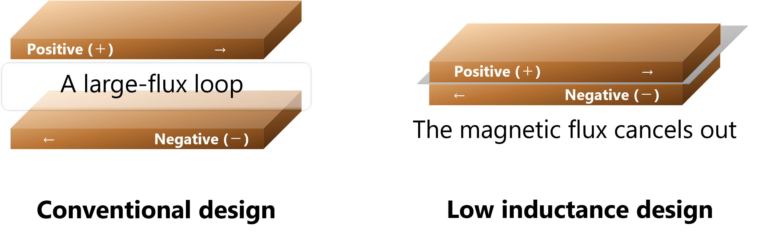
Place the Forward and Return Paths Opposite Each Other
The most fundamental way to reduce inductance is to place the forward and return current paths as close together as possible in opposing layers. When these paths overlap, their magnetic fields largely cancel each other, minimizing the effective current loop area.
This approach effectively lowers parasitic inductance and helps suppress overvoltage and noise during high-speed switching.
Minimize the Distance Between Layers
As the distance between conductor layers increases, the current loop area also increases, raising the inductance. Therefore, it is important to minimize the distance between layers while maintaining sufficient insulation performance.
By using thin insulating materials to position the conductors closer together, it is possible to achieve both low inductance and high-voltage insulation capability.
Maximize the Overlap Area
Increasing the overlap area between the forward and return conductors also reduces inductance. A larger overlap strengthens magnetic coupling and suppresses loop inductance.
Designers should therefore optimize conductor shape and layout to maximize overlap in laminated busbars.
Insert Molding Technology for Low-Inductance Laminated Busbars
Having established why low inductance matters and how busbar geometry influences it, we now introduce an advanced insert molding technology developed by NAGASE Mobility that pushes these principles further.
In conventional injection molding, resin flow characteristics have limited the minimum conductor spacing to approximately 0.5 mm. NAGASE Mobility has overcome this constraint by developing a process that integrates a 0.1-mm-thick resin-insulating film directly with the busbar during molding, achieving approximately 30% lower inductance than conventional designs.

Rather than simply inserting the insulating film between busbars, this method introduces a primary molding step that first encapsulates the film with resin. This preliminary encapsulation prevents film misalignment or damage during the subsequent molding process, ensuring consistent quality at production scale.
By integrally molding the insulating film and busbar, it is possible to further reduce the distance between conductors while maintaining high insulation reliability and achieving an ultra-low-inductance structure.
Beyond inductance reduction, this integrated molding technology also benefits thermal management and cooling design. As busbars become thinner and handle higher voltages and currents, this process supports designs that minimize the thermal path to cooling surfaces and incorporates structures optimized for heat resistance.
This technology represents a proven approach to achieving ultra-low-inductance laminated busbars and is particularly well-suited for next-generation EV and HEV power electronics platforms .
Insert Molding for Automotive Components – NAGASE Mobility
For components such as laminated busbars—which involve electrical challenges, such as inductance reduction, and may also include complex geometries—it is important to consider design, materials, and manufacturing processes together. In particular, when developing components for mass production, designers must address not only performance but also manufacturability and consistent product quality.
NAGASE Mobility provides design proposals and technical support for parts with specialized requirements, such as inductance control, complex geometries, or multi-step manufacturing processes, with a focus on enabling efficient mass production.
Insert Molding for Power Modules | NAGASE Mobility | NAGASE
Beyond insert molding technology itself, NAGASE Mobility offers comprehensive support that spans the full product lifecycle:
Selecting optimal resin materials based on application and performance requirements
Evaluating manufacturing processes with mass production in mind
Developing supply chains to ensure stable production.
This approach enables us to deliver integrated solutions from technical development to mass production launch.
If you can share drawings or specifications, our engineering team can propose solutions tailored to your specific challenges and applications. For inquiries regarding insert molding for automotive components, please feel free to contact us.