Resources ~ DENATRON Museum ~ / Get to know DENATRON
Semiconductor Process Tapes in Advanced Wafer Processing
HOME > Resources ~ DENATRON Museum ~ > Get to know DENATRON > Semiconductor Process Tapes in Advanced Wafer Processing
- What is the Semiconductor Process Tape?
- Types of Semiconductor Tapes
- Requirements for Semiconductor Tapes
- Antistatic Film: DENATRON
Semiconductor manufacturing is a process involving numerous steps, each requiring specialized materials. Among these, semiconductor process tapes are often overlooked, as they are discarded after use. However, these tapes play an indispensable role in ensuring stable and reliable manufacturing processes.
This article provides a detailed overview of the semiconductor process tapes used in dicing and back-grinding (wafer backside grinding) processes.
What is the Semiconductor Process Tape?
Semiconductor process tapes are specialized adhesive tapes primarily used in dicing and back-grinding processes during the manufacture of semiconductor devices such as central processing units and memory chips.
In recent years, the demand for thinner electronic devices, such as smartphones and personal computers, has driven the need for thinner semiconductor chips. As a result, back grinding has become an essential process, further increasing the importance of semiconductor process tapes.
Supporting Device Thinning and 3D Packaging Technologies
In 3D packaging technologies, where chips are stacked vertically, extremely thin semiconductor chips are required to reduce the overall package height.
Back-grinding is an essential process for this thinning, and semiconductor process tapes play a critical role in ensuring stable wafer handling throughout the procedure.
Role in the Dicing Process
During the dicing process—where a wafer is cut into individual chips—process tape is applied to the backside of the wafer to prevent chips from scattering during cutting. This contributes to improved yield and overall manufacturing efficiency.
Thus, semiconductor process tapes are an indispensable material in semiconductor manufacturing.
Types of Semiconductor Tapes
There are several types of semiconductor process tapes. In this section, four representative types are introduced.
Ultraviolet-Curable Tape
Ultraviolet-curable tapes are designed to lose their adhesive strength upon ultraviolet (UV) irradiation. Before UV exposure, they provide sufficient adhesion to securely hold the wafer. After the process is complete and the tape is no longer required, it can be easily removed by UV irradiation.
In general, the adhesives used in UV tapes are composed of materials known as base polymers and oligomers. Before UV irradiation, fluid oligomers are dispersed within a base polymer with a network structure; this combination provides the adhesive properties of the tape.
When UV light is applied, the oligomers undergo a cross-linking reaction and bond together to form a new network structure. As a result, a dual-network structure consisting of both the base polymer and the oligomers is created, causing the adhesive to harden and lose its tackiness.
Thermal Release Tape (Heat-Releasable Tape)
Thermal release tapes are specialized tapes in which the adhesive softens and loses its bonding strength when heated. At room temperature, they provide sufficient adhesion to securely attach to substrates such as wafers. After the process is complete, the tape can be easily removed by applying heat.
Dicing Tape
Dicing tapes are used in the dicing stage of semiconductor manufacturing. By applying the tape to the back side of the wafer prior to dicing, the process can be carried out safely and efficiently.
Dicing tapes are commonly blue in color, and UV-type tapes, which reduce adhesive strength upon UV irradiation during debonding, are widely used.
The dicing process involves cutting a wafer by applying a rotating, disk-shaped dicing saw (with a diamond blade) from the front side of the wafer. By moving the blade in the X and Y directions, the wafer is separated into individual chips.
Without a dicing tape applied to the back side of the wafer, the separated chips can scatter during cutting. For this reason, dicing tapes are indispensable for maintaining yield.
Back-Grinding Tape
Back-grinding tapes are used in the polishing stage—known as the back-grinding process—in semiconductor manufacturing. To protect the wafer surface where circuits are formed, the back side of the wafer is ground while the tape is applied to the front side prior to polishing.
Back grinding is a process in which the back side of a wafer is thinned using chemical or mechanical methods. During this process, significant mechanical stress is applied to the wafer, creating risks such as chipping and cracking. In addition, preventing contamination from foreign particles generated during grinding is also critical.
To mitigate these issues, back-grinding tapes are indispensable.
Back-grinding tapes can be classified into two types based on their debonding methods:
・UV type: The adhesive strength is reduced by UV irradiation, allowing for easy removal.
・Non-UV type: The tape is removed using methods other than UV irradiation, such as heat.
Selecting the appropriate type based on application and process conditions is essential.
Requirements for Semiconductor Tapes
Semiconductor process tapes must satisfy a broad range of performance criteria. They must endure rigorous manufacturing conditions without adversely affecting the cleanroom environment or the final product. The most critical performance factors are outlined below.
Adjustability of Adhesive Strength
A primary requirement for semiconductor process tapes is the ability to provide both high-tack adhesion and effortless removability, depending on the specific manufacturing stage.
During back-grinding and dicing, sufficient adhesive strength is essential to secure the wafer firmly. However, once the process is complete, the tape must be easily removed without causing mechanical damage or leaving residue on the wafer. The ability to precisely tune adhesive strength—often via UV irradiation or thermal triggers—is a defining characteristic of high-quality semiconductor process tapes.
Heat Resistance
In addition to polishing and dicing, there are process steps in which tapes remain applied while being exposed to high temperatures. Examples include:
・Drying after cleaning (vacuum drying)
・Reflow processes used to form bumps (solder balls) on semiconductor chips
In these processes, tapes must withstand temperatures of approximately 150°C to 260°C. If its heat resistance is insufficient, the tape may peel off or melt, creating a risk of contamination as it mixes with the solder.
Low Residue (Low Contamination)
Because semiconductor circuits are fabricated at the nanometer scale, any adhesive residue left on the wafer during tape removal can cause contamination, leading to defects such as short circuits and open circuits.
Peelability (Workability)
Easy tape removal after processing is also an important requirement. If excessive adhesive strength remains, excessive force may be applied to the wafer during debonding, potentially causing warpage or damage.
In addition, tape removal is typically automated, and debonding performance has a direct impact on takt time. To achieve a short turnaround time, defined as the time from when a wafer enters a tool until the time it exits, good debonding characteristics are essential.
Electrostatic Protection (Antistatic Performance)
Since semiconductors are composed of electronic circuits, the accumulation of static electricity can cause unintended current flow, potentially leading to short circuits. This, in turn, reduces chip yield and negatively impacts manufacturing costs and profitability.
For this reason, semiconductor process tapes used in semiconductor manufacturing must possess antistatic properties that prevent the buildup of static electricity. Such properties are essential for ensuring product reliability and maintaining high yield.
Cleanroom Compatibility
Because semiconductor manufacturing is highly sensitive to microscopic contamination, especially in front-end processes, these operations are carried out in cleanrooms.
As a result, semiconductor process tapes must meet the following criteria:
・They must not generate particles or dust.
・Outgassing, particularly the release of volatile gases, must be minimized.
Since volatile organic compounds can lead to product defects, low outgassing performance is especially critical.
Antistatic Film: DENATRON
Nagase ChemteX provides conductive coating materials (antistatic agents) designed for use in semiconductor manufacturing. These products play an important role in preventing defects caused by static electricity.
Overview
One of the causes of defects in semiconductor manufacturing is static electricity. The key to preventing defects is not to eliminate static electricity after it has accumulated but to prevent its buildup preemptively.
Nagase ChemteX’s conductive coating materials incorporate either conductive polymers (PEDOT:PSS) or carbon nanotubes (CNTs), providing high reliability and safety.
Applications
In semiconductor manufacturing, tapes are used not only in dicing and back-grinding processes but also in other stages of handling and transportation.
Because semiconductor chips are extremely small, transporting them as individual pieces is difficult. Instead, they are placed in pocket-shaped holders, known as carrier tapes, for transportation.
To prevent chips from falling out of carrier tapes, sealing is required. The tape used for this sealing is called a cover tape, and it has been treated with Nagase ChemteX’s conductive coating materials.
Applicable Products
Two types of conductive coating materials (antistatic agents) suitable for use on cover tapes are described below.
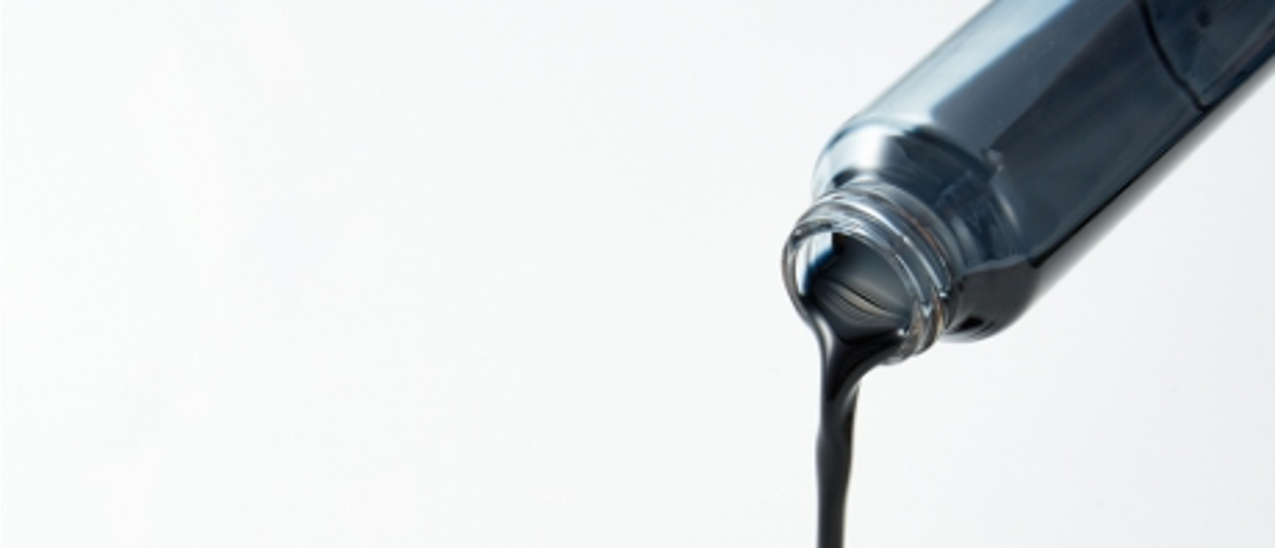
P-560ST
This coating material is based on the conductive polymer PEDOT:PSS and offers excellent stretchability. Its primary solvent is water, making it suitable for in-line coating processes. It also exhibits good adhesion to various substrates.
In addition to its use in cover tapes, it also has antistatic applications in optical films and industrial materials. Additionally, it demonstrates excellent storage stability, remaining stable for up to 12 months at 5°C, allowing unused material to be stored for a certain period.
Table 1. Liquid properties of P-560ST
Please scroll horizontally.
| Appearance | Dark blue |
|---|---|
| Main components | Conductive material, stretchability modifier |
| Primary solvent | Water |
| pH | 6〜9 |
| Viscosity | 10〜30mPa・s |
| Storage stability (5°C) | 12 months |
| Storage stability (25°C) | 4 months |
C-100A
This is a transparent antistatic coating material based on CNTs. It adheres well to a wide range of substrates, including polyethylene terephthalate, polymethyl methacrylate, polyamide, and acrylonitrile butadiene styrene, and exhibits outstanding durability where heat resistance and resistance to humid heat are concerned.
Similar to P-560ST, it offers an outstanding shelf life of 12 months when stored at 5°C. This ensures that any remaining material can be safely stored and reused over an extended period.
In addition to its use in cover tapes, it also has antistatic applications in optical films and industrial materials.
Table 2. Liquid properties of C-100A
Please scroll horizontally.
| Appearance | Black |
|---|---|
| Main components | Conductive material, binder resin |
| Primary solvent | Water |
| pH | 6-10 |
| Viscosity | 5-10 mPa・s |
| Storage stability (5°C) | 12 months |
| Storage stability (25°C) | 4 months |
Return to list of articles